Cost-effective, Simplified IoT Hardware Design Achieved with Winbond SpiStack Flash Memory

With the offering of the Winbond W25M Series of SpiStack Flash memory, designers of small IoT and M2M (machine-to-machine) hardware devices no longer need to make the tradeoff of selecting NOR over NAND flash memory, or simple over complex PCB board design to incorporate design layouts for both kinds of memory. The W25M Series includes options for both homogeneous (NOR+NOR or NAND+NAND Flash memory dies) and heterogeneous stacked SpiFlash dies (NOR+NAND Flash memory dies). The NOR Flash memory densities range from 1 MB to 256 MB, while the NAND Flash memory densities range from 512 MB to 2 GB. The range of options gives designers ultimate flexibility in achieving the ideal Flash memory densities for both code storage and data storage for their hardware product development needs.
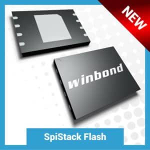
Winbond offers the W25M Series in the industry-standard 8-pin 8x6mm WSON package and features the well-established multi-IO SpiFlash interface and command set, both, with which designers are familiar and comfortable. The compact package of the W25M aides both the design of small devices and with a low pin-count reduces the complexity of the board design and the provision of interfaces with the SoC (system-on-chip) or MCU (microcontroller). This reduces CS (Chip Select) command lines, thus traces on the board, to the SPI bus and the requirements for the added interface pin-count from the SoC that typically are needed from other memory solutions that require dedicated CS lines for each die.
In contrast to typical solution mentioned above that requires two, or more, memory packages, enabled by hardware and more complex board design, the W25M Series achieves simplicity in board design through a compact, stacked Flash memory package enabled through software. The software Chip Select feature in the W25M series functions over one CS channel between the memory package and the SoC. Easy Chip Select commands notify the memory dies – each die is identified by a unique factory-assigned ID – which one is to occupy the SPI bus. As a result, the Winbond SpiStack solution produces a reduction in board size and complexity over the typical board layout design that requires the accommodation of two Flash memory packages and their interfaces to the SoC or MCU. 16-pin SOIC or 24-pad BGA package options in the W25M Series, provide additional board design flexibility.
The two Flash memory dies making up the stacked SpiFlash W25M solution have clock rates up to 104 MHz and provide even higher performance when employing Quad-SPI for an equivalent of 416 MHz (a 50 MB/s transfer rate). The high-bandwitdh enables Read/Write operations between the Flash memory and SoC or MCU, supporting the execution of code (XIP) directly from the Flash memory die in the W25M Series without shadowing it to DRAM. Thus, the need for DRAM is eliminated from the hardware design.
Furthermore, SpiStack supports concurrent operations – read operations on one die and write/erase operations on the other die – so that code execution is not interrupted for the updating of data. The combination of concurrent processes is ideally suited for applications that require the high reliability of code storage (integrating high endurance and retention with fast random access time) offered by NOR Flash memory and cost-effective, high-density NAND Flash memory for data storage and boot code backup. The heterogeneous stacked NOR plus NAND Flash memory dies provided in the W25M Series best supports such an application.
Hardware designers can implement the W25M Series in a wide range of consumer and enterprise applications from mobile phone, camera, printer, server, set-top box, Bluetooth, GPS, Digital/Smart TV, DSP, FPGA, WLAN, DSL/Cable Modem, to IoT gateway/node and wearable, etc. to market vertical from automotive and transportation, to health, communication, agriculture, construction, and energy. Additionally, low power and wide-temperature range (-40°C to +85°C) features enable the Series to be used in hardware designs to meet the challenges of industrial, mission-critical applications in harsh environments.
The SpiStack W25M Memory Series is currently available or underdevelopment with the following Flash memory density combinations:
• 128 MB Serial NOR + 1 GB Serial NAND
• 16 MB Serial NOR + 1 GB Serial NAND
• 16 MB Serial NOR + 512 MB Serial NAND
• 32 MB Serial NOR + 1 GB Serial NAND
• 64 MB Serial NOR + 1 GB Serial NAND
The Winbond W25M Series of SpiStack flash memory provides a multitude of combinations NOR and NAND Flash memory stacking options most appropriate to fit the needs of hardware device design for any application or market vertical. This is especially critical for hardware product designers with very particular design needs for IoT applications where board simplicity and device size requirements are paramount for creating their ideal device. At the same time, they can reduce BOM costs and board redesign spin and ultimately bring their product to market on time and budget. For further information about where to buy a W25M Series SpiStack solution, please check Winbond Official eStore on TechDesign.


